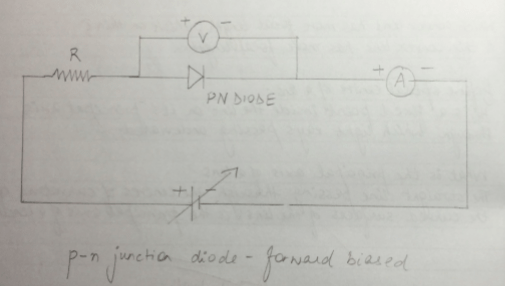
P N Junction Circuit Diagram
Easy way technical point: p-n junction Junction forward bias formation voltage type physics definition potential connected characteristics application Pn junction theory
3: p-n junction When a metallurgical junction is formed between an n
Draw the circuit arrangement for studying v-i characteristics of a p-n Junction pn theory electrical4u between make interface 3: p-n junction when a metallurgical junction is formed between an n
Diode junction schematic symbol pn forward biased type semiconductor silicon curve vs characteristic technocrazed arrow semiconductors corresponding electronics device advertisement
Working principle of p-n junction in forward bias conditionJunction pn potential diode semiconductor theory region depletion between distance gif type diffusion doping voltage difference barrier semiconductors basic welcome Junction minor conditionsWhat is p-n junction?.
Cbse biology practical class xiiBias junction biased diode Junction circuited appliedPn formation diode forming.

Diode forward junction bias types pn reverse diodes biased under electrical4u type electrons semiconductor symbol current circuit diffusion explained physics
Forward and reverse bias of p n junctionPn junction: formation & structure Reverse circuit junction pn forward diagram biased bias diodeAn introduction to p-n junction diode and its working.
☑ pn junction at equilibriumPn junction: what is it? (and how to make one) Pn junctionWhat is reverse bias p n junction?.

Junction bias biasing reverse
Junction biasJunction diode band diagram forward energy bias pn reverse characteristics difference voltage tunnel between if lekule apply across then The current through an ideal p–n junction shown in the circuit diagramPn junction theory for semiconductor diodes.
Junction working forward bias principle barrier potential condition electrical depletion widthDiode bias biased across pn applied varactor semiconductor diodes circuits Diode junction forward biasing diagram circuit characteristics practical resistance graph dynamic state drawing find classWhat is an open-circuited p-n junction?.

P-n junction diode and characteristics of p-n junction
What happens when a pn junction diode is forward biasedJunction circuit ideal sarthaks Pn semiconductor diffusion drift equilibrium chapterCircuit diagram of pn junction in reverse biased and forward biased.
Junction bias draw studying arrangement pn diode reverse obtaining reversed2.6 the p-n junction Forward reverse pn junction circuit diagram bias biased diodeJunction forward depletion region diagram biased pn including showing figure.

Metallurgical semiconductor formed diffusion charge drift electric carrier
Junction diode forward working bias pn biasing its reverse voltage introductionCircuit diagram of pn junction in reverse biased and forward biased Diode pn junction ppt presentation powerpoint slideserve bollenP-n junction.
.